High-Speed Copper Reach Limits & Signal Integrity Degradation at PCIe 6.0/7.0
The migration to PCIe 6.0 and PCIe 7.0 specifications introduces fundamental physical barriers across electrical copper interconnects. Operating at 64 GT/s and 128 GT/s requires transition from non-return-to-zero (NRZ) to 4-level pulse amplitude modulation (PAM4), which halves the Nyquist frequency to 16 GHz and 32 GHz respectively, but at the cost of dividing the eye height by three. Consequently, channel insertion loss escalates exponentially due to dielectric absorption (governed by the substrate dissipation factor) and skin-effect surface resistivity. Across ultra-low-loss PCB laminates such as Megtron 8 and high-gauge passive Direct Attach Copper (DAC) cables, the standardized Nyquist loss budget of 32 dB to 36 dB is consumed within 0.8 to 1.0 meters of physical run. This spatial confinement forces accelerators, host processors, and fabric switches into dense, localized physical configurations, eliminating the architectural flexibility required by modern AI scale-up systems.
To mitigate passive loss, hardware designers have historically relied on Active Electrical Cables (AEC) and intermediary PCB retimers. However, the electrical penalties of active copper devices at 128 GT/s become self-defeating at scale. A typical x16 PCIe 6.0 retimer consumes between 2.0W and 3.5W per physical lane, introducing tens of watts of parasitic thermal dissipation inside an already dense compute sled. Concurrently, the intrinsic Signal-to-Noise-and-Distortion Ratio (SNDR) degrades by roughly 9.5 dB under PAM4, mandating complex Continuous Time Linear Equalization (CTLE), multi-tap Feed Forward Equalization (FFE), and Decision Feedback Equalization (DFE). The resulting Bit Error Rate (BER) hovers near the 10^-6 boundary before Forward Error Correction (FEC), demanding computationally intense lightweight FEC decoding. At 128 GT/s, structural return loss, high-density pinout crosstalk (NEXT and FEXT), and intra-pair skew in twinaxial copper wires introduce uncorrectable Flit errors, effectively exhausting the scalability of copper interconnects.
Enforce strict insertion loss ceilings of 32 dB at 16 GHz (PCIe 6.0) and 36 dB at 32 GHz (PCIe 7.0) across all electrical trace budgets.
Quantify pre-FEC Bit Error Rate thresholds (< 10^-6 for PAM4) across host channels to avoid uncorrectable Flit replays.
Restrict passive copper DAC reach to < 1.0 meter and cap active retimer thermal budgets at 2.5W per physical lane.
Optical PCIe Architecture & Multi-Channel VCSEL Transceiver Dynamics
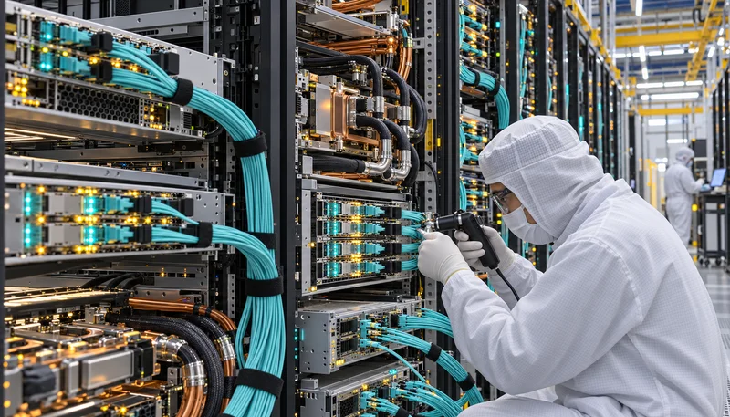
Optical PCIe represents an architectural transition that decouples physical link reach from protocol performance, preserving native PCI-SIG protocol semantics across optical waveguides. Unlike Ethernet or InfiniBand, which operate through multi-layered packet encapsulation and transport protocols, Optical PCIe maintains raw transaction layer packet (TLP) structures, Flit-mode framing, credit-based flow control, and load/store memory-mapped I/O coherency without protocol translation. The physical implementation relies on Vertical-Cavity Surface-Emitting Laser (VCSEL) arrays transmitting over 850 nm and 910 nm dual-wavelength OM4 or OM5 bend-insensitive multimode fiber ribbons. High-speed transceivers driven by low-power, analog-direct-drive driver ICs map PAM4 electrical lanes directly to the optical domain, extending native interconnect distance from less than 1.5 meters to 10 to 100 meters throughout the data hall.
The primary design constraint in optical PCIe transmission is preserving the ultra-low latency profiles critical for PCIe and Compute Express Link (CXL) cache-coherent memory semantics. Advanced optical engines deploy direct analog modulation topologies that achieve electro-optical-electro (E-O-E) conversion latencies of less than 5 nanoseconds per direction, entirely bypassing the multi-clock-cycle latencies inherent to full digital signal processing (DSP) retimers. By constraining optical transport latency to approximately 5 ns per meter of fiber, coherent clusters can span multiple server cabinets while comfortably remaining within standard PCIe retry buffer timeouts and CXL.mem transaction windows. This optical transparency enables high-radix fabric switches—such as Astera Labs Scorpio—to orchestrate peer-to-peer data transfers between disaggregated compute and pooled CXL memory blocks across the data center with zero software intervention.
Validate bidirectional Electro-to-Optical-to-Electrical conversion latency does not exceed 5.0 ns.
Deploy 850/910 nm multi-channel VCSEL optical engines over OM4/OM5 bend-insensitive multimode fiber ribbons.
Verify PCIe ACK/NAK retry buffer timers accommodate optical propagation delay across target cable lengths (up to 100 meters).
Rack-Scale Compute Disaggregation & Scale-Up AI Cluster Topology
The rigid spatial coupling of GPUs, high-bandwidth memory, CPUs, and networking within homogeneous server sleds has created critical scaling bottlenecks in enterprise AI infrastructure. High-TDP accelerator complexes routinely exceed the thermal dissipation and power delivery limits of standard 19-inch and 21-inch Open Rack Standard (ORV3) envelopes. Optical PCIe enables rack-scale compute disaggregation by breaking the physical proximity requirement between accelerator complexes, Smart Switches, and disaggregated memory/CXL storage pools. Accelerators can reside within specialized compute sleds that maximize thermal volume, while high-radix optical PCIe fabric switches dynamically aggregate remote CXL memory sleds into unified, shared address spaces across multi-rack scale-up domains.
By extending the scale-up domain from a single chassis of 8 GPUs to multi-cabinet pods encompassing 64, 128, or 256 accelerators, system architects bypass localized power density limits without incurring the software fragmentation of standard scale-out networking. Furthermore, the physical replacement of heavy, rigid copper harnesses with micro-diameter optical fiber bundles completely transforms rack rear management. Eliminating dozens of dense copper cables running across server exhaust panels liberates valuable volume within the hot aisle, restores unobstructed airflow pathways, and eliminates the severe mechanical stress exerted on backplane connectors by heavy copper wire bundles.
Architect disaggregated CXL 3.1 pooling across optical fabric switches supporting scale-up domains of at least 64 endpoints.
Replace rear-chassis copper cable bundles with compact fiber harnesses to maximize hot-aisle exhaust volume.
Configure automated PCIe fabric managers to dynamically provision pooled memory capacity to GPU compute sleds on demand.
Power Dissipation, Thermal Airflow Impedance & Interconnect Efficiency
Thermal management in modern 100 kW+ AI racks is heavily impacted by parasitic airflow impedance at the chassis rear. Passive and active copper cable bundles historically obstructed up to 40% of the chassis exhaust plane, creating significant air backpressure. This impedance forces internal pulse-width-modulated (PWM) cooling fans to operate continuously at high duty cycles, consuming up to 15% to 20% of total server power solely to overcome flow resistance. Optical interconnects fundamentally eliminate this parasitic thermal impedance: high-density optical fiber ribbons occupy less than 10% of the cross-sectional area of equivalent copper bundles, immediately restoring laminar exhaust pathways and slashing cooling fan power draw across the subrack.
At the silicon level, the energy consumption trade-offs increasingly favor optical PCIe engines as data rates hit 64 GT/s and 128 GT/s. An active electrical channel driven by multi-stage retimers requires substantial power (2.5W to 3.5W per x1 lane), generating concentrated heat directly on the PCB. In contrast, advanced direct-drive mid-board optics (MBO) and co-packaged optics (CPO) operate with energy budgets below 8 to 10 pJ/bit. Furthermore, optical architectures enable thermal isolation: by placing the sensitive optical engines on dedicated mid-board carrier locations or front-panel assemblies separated from the primary ASIC thermal zone, optical laser diodes are protected from the extreme thermal soak (> 100°C) of the accelerator heat sinks, keeping VCSEL junction temperatures within the optimal 70°C reliability envelope.
Audit chassis exhaust static pressure drop, targeting airflow impedance reductions > 35% compared to copper cabling.
Enforce interconnect power efficiency targets strictly under 10 pJ/bit for optical transceivers operating at 64 GT/s PAM4.
Implement thermal isolation zones separating optical VCSEL engines from high-TDP accelerator heat sinks.
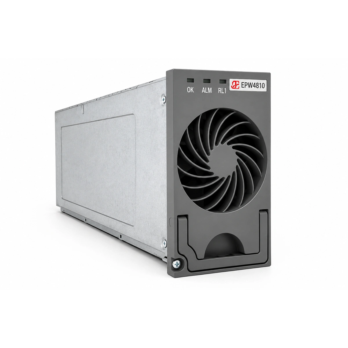
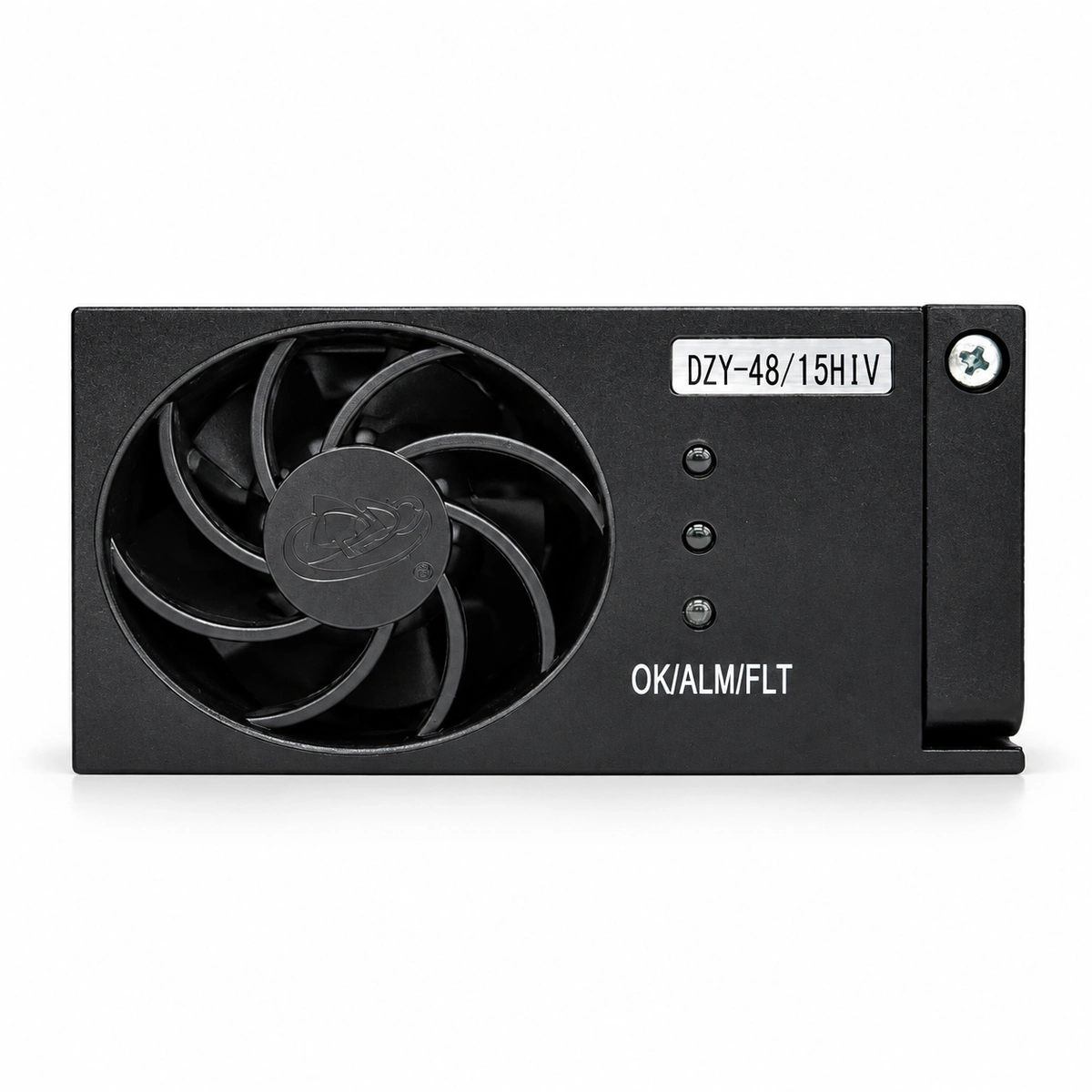
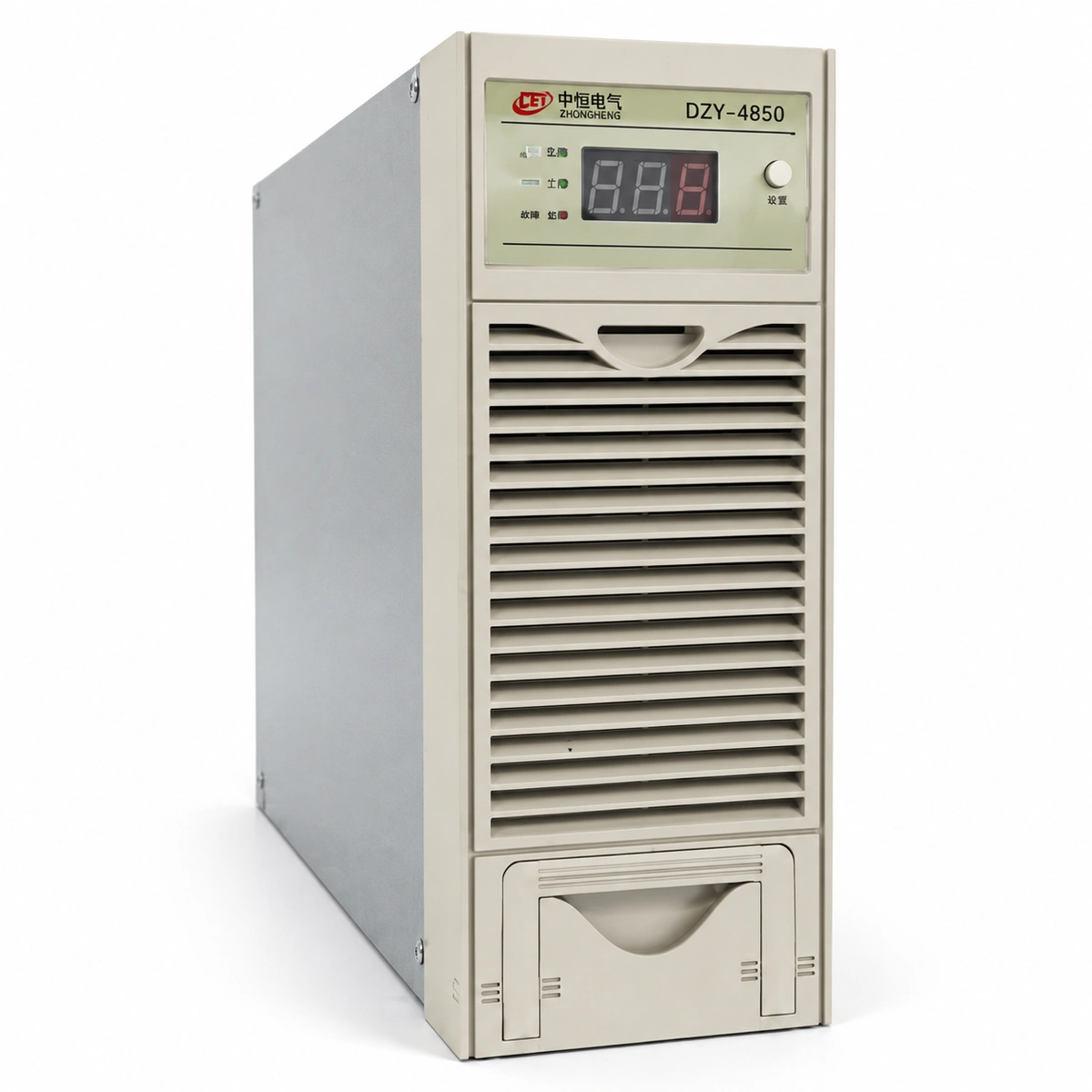
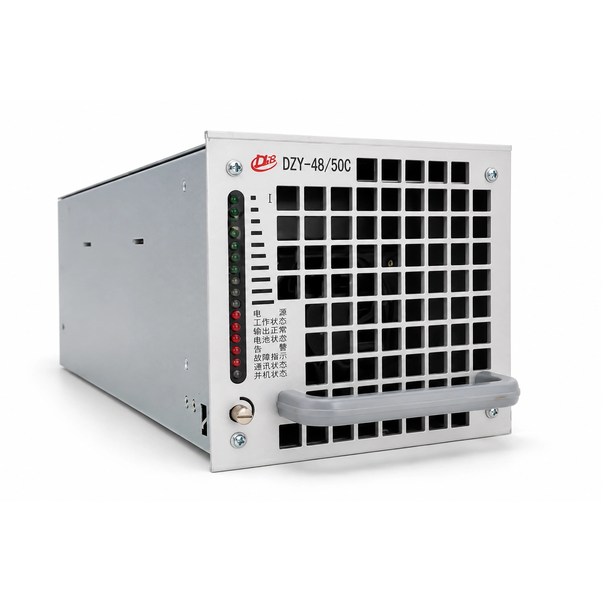
Subrack DC Power Distribution & High-Availability Power Backing
The operation of distributed, high-radix optical PCIe fabrics requires uncompromising power integrity across every subrack. Integrating disaggregated optical switches, PCIe expansion sleds, and high-power compute nodes necessitates a centralized -48V or 54V DC busway architecture, displacing fragmented AC-to-DC power supplies within individual chassis. Direct DC busbar distribution eliminates multiple internal power conversion stages, elevates power delivery efficiency, and establishes a single low-impedance ground reference across adjacent racks. This unified ground reference prevents ground potential shifts between chassis, which can otherwise introduce common-mode noise and disrupt high-speed signal integrity across multi-rack systems.
Because native PCIe protocol links cannot tolerate deep packet-retransmission stalls, optical link state transitions must remain fully resilient against power disturbances. Microsecond transient loads—such as when multiple optical engines and accelerator cores transition synchronously between dynamic power states (L0 to L0s/L1 and back)—generate severe di/dt voltage spikes. To prevent fabric partitioning or link-drop resets, high-availability subrack power architectures integrate redundant N+1 or 2N rectifier shelves, local Battery Backup Units (BBU) capable of 15 ms bridge times, and distributed multiphase point-of-load (PoL) regulators designed to hold the DC bus within a tight ±2% tolerance under instantaneous full-load steps.
Deploy continuous -48V / 54V DC solid busbars across all subracks supporting optical switch and compute sleds.
Verify subrack DC-DC point-of-load regulators maintain bus voltages within ±2% during worst-case di/dt step loads.
Integrate distributed subrack Battery Backup Units (BBUs) with zero-transfer-time solid-state automatic transfer switches.
Standardization, MPO Fiber Connector Reliability & Field Maintenance Protocols
Scaling optical PCIe from enterprise proof-of-concept demonstrations into mainstream hyperscale production relies on rigorous industry standardization led by the PCI-SIG Optical Workgroup and the Open Compute Project (OCP). Standardization frameworks establish interoperable physical layer specifications, protocol-aware sideband management, and uniform mechanical interfaces such as OSFP-XD and high-density blind-mate optical backplanes. Unlike enclosed copper pins, optical connections are vulnerable to microscopic particulate contamination. Even a single 1-micron dust particle resting on a multi-fiber push-on (MPO/MTP) ferrule core can induce unacceptable insertion loss spikes, high back-reflection (ORL), and localized signal clipping on PAM4 links.
Achieving an enterprise Mean Time Between Failures (MTBF) exceeding 10^7 hours across thousands of multi-channel VCSEL laser arrays requires deterministic field maintenance workflows and telemetry. Automated digital inspection microscopes with automated pass/fail scoring compliant with IEC 61300-3-35 must be standard tooling during installation and servicing. Furthermore, next-generation optical switches incorporate onboard optical power telemetry, continuously tracking parameters including laser bias currents, receiver Optical Signal-to-Noise Ratio (OSNR), and pre-FEC Bit Error Rates. Streaming these parameters to centralized AIOps telemetry platforms enables predictive maintenance, triggering automated live migrations of PCIe workloads before physical link degradation causes silent data corruption or cluster timeouts.
Adopt PCI-SIG Optical Workgroup and OCP standardized blind-mate optical backplane connector form factors.
Mandate automated IEC 61300-3-35 fiber endface digital inspection and cleaning protocols prior to any optical mating.
Configure streaming telemetry for real-time tracking of VCSEL bias current, RSSI, and pre-FEC error rates to execute predictive hot-swaps.
Engineering Procurement & Technical Desk
For technical datasheets, custom power topology design, or volume export quotations, reach out to RICEWIND engineers.