The Pluggable Optics Thermal and SerDes Power Wall at 102.4Tbps
Horizontal scale-out architectures in modern artificial intelligence clusters demand non-blocking, high-radix switch fabrics connecting tens of thousands of compute accelerators. In traditional switch topologies utilizing 800G and 1.6T front-panel pluggable transceivers (OSFP and QSFP-DD), aggregate bandwidth scaling to 51.2Tbps and 102.4Tbps encounters an intractable channel insertion loss barrier. At 106.25 Gbps and 212.5 Gbps PAM4 per lane, host SerDes circuits driving electrical traces across Megtron 7 or advanced Megtron 8 PCB laminates suffer high-frequency signal attenuation exceeding 28 to 32 dB over distances of 10 to 14 inches. Overcoming this severe frequency-dependent dielectric and skin-effect loss requires heavy digital signal processors (DSPs) with aggressive continuous-time linear equalization (CTLE) and decision feedback equalization (DFE), consuming massive silicon real estate and electrical power.
This architectural paradigm drives optical interconnect energy consumption to unsustainable levels of 18 to 22 pJ/bit. Inside a 1RU or 2RU 102.4Tbps switch chassis, the front-panel optical transceivers alone account for 1,800W to 2,200W, pushing total system chassis power beyond 4,500W. The resulting thermal flux at the front bezel creates catastrophic cooling bottlenecks; forced-air thermal convection reaches physical velocity limits, leading to transceiver junction temperatures exceeding 85°C. This elevated thermal stress degrades vertical-cavity surface-emitting lasers (VCSELs) and electro-absorption modulated lasers (EMLs), while generating unmanageable acoustic noise and stranded power across hyperscale data center facilities.
Cap electrical trace insertion loss between switch ASIC SerDes and optical engine below 6 dB at 53.125 GHz Nyquist frequency.
Restrict per-port transceiver electrical power consumption to less than 10 W per 800G equivalent interface.
Eliminate front-panel thermal choke points by transitioning from forced convection cooling to direct-to-die liquid architectures.
Co-Packaged Optics (CPO) Silicon Photonics Engine Architecture (<7 pJ/bit vs 20 pJ/bit)
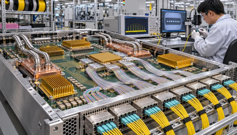
Co-Packaged Optics bypasses the electrical trace attenuation barrier by monolithically or heterogeneously integrating silicon photonics (SiPh) optical engines onto the same organic multi-chip module (MCM) substrate or high-density silicon interposer as the high-radix switch ASIC (such as 102.4Tbps architectures). In a standard 32 x 3.2T optical engine topology, electrical interconnect distances between the switch SerDes and the optical engine transmitter/receiver analog front ends are compressed from 300 mm down to 15 to 25 mm. This drastic physical reduction enables the deployment of Linear Direct-Drive interfaces, completely eliminating the power-hungry retimer DSP chips traditionally embedded inside pluggable modules.
Removing retimer DSPs reduces total interconnect energy consumption from ~20 pJ/bit down to 5–7 pJ/bit, representing a net power reduction exceeding 65%. The 3.2T optical engines leverage high-density 2.5D packaging combining ultra-low-loss dielectric polymer waveguides, sub-micron silicon waveguides, and arrays of silicon Mach-Zehnder Modulators (MZMs) or micro-ring modulators (MRMs). Modulated optical signals are coupled off-chip via high-efficiency sub-wavelength grating couplers or inverted edge tapers into high-density 2D optical fiber ribbons terminating at multi-fiber push-on (MPO-16, MPO-24, or MXC) blind-mate optical connectors.
Verify analog direct-drive SerDes-to-modulator path maintains total channel loss below 3.5 dB across all 32 lanes per 3.2T engine.
Enforce strict optical engine energy efficiency metrics not to exceed 6.5 pJ/bit across typical operating temperature profiles.
Ensure silicon photonics grating coupler or edge facet coupling loss remains strictly under 1.2 dB per optical interface at 1310 nm.
The ELSFP Remote Laser Architecture: Indium Phosphide MTBF and Hot-Swappable Laser Safety
A foundational challenge in Co-Packaged Optics design is the acute thermal vulnerability of Indium Phosphide (InP) Continuous Wave (CW) laser diodes. When laser diodes operate above 55°C to 65°C, their threshold current increases exponentially, optical slope efficiency degrades precipitously, and thermo-mechanical degradation mechanisms accelerate, slashing Mean Time Between Failures (MTBF) from millions of hours down to tens of thousands of hours. Because a monolithic 102.4Tbps switch ASIC operates at silicon junction temperatures between 85°C and 105°C, co-packaging laser diodes directly on the MCM package substrate would cause catastrophic, cluster-wide optical link failures and impossible board repair procedures.
The OIF External Laser Small Form-Factor Pluggable (ELSFP) standard resolves this thermal mismatch by decoupling the continuous-wave Distributed Feedback (DFB) laser sources from the central multi-chip module. High-power ELSFP modules (delivering +20 to +24 dBm optical launch power across multiple channels) are mounted on the cooler front chassis bezel or within a dedicated external laser rack shelf. Optical power is delivered to the silicon photonics modulators via polarization-maintaining fiber (PMF) arrays. This enables zero-downtime hot-swapping of failed laser modules without disturbing the 102.4Tbps switch ASIC, while onboard Class 1 eye-safety microcontrollers execute automatic laser shutdown (ALS) within 100 milliseconds of any un-mating event.
Maintain ELSFP laser case operating temperatures strictly below 50°C using isolated front-panel airflow channels.
Verify polarization-maintaining fiber (PMF) polarization crosstalk extinction ratio exceeds 20 dB over environmental thermal cycles.
Validate hardware-level Automatic Laser Shutdown (ALS) latency under 100 ms upon connector disengagement to satisfy Class 1 laser safety.
High-Radix Fiber Management, Optical Link Loss Budgets, and Cleanliness
Integrating a 102.4Tbps CPO switch requires routing unprecedented optical fiber densities within a compact chassis. A fully configured system utilizes 32 optical engines operating at 3.2Tbps, demanding the precise management of 512 to 1,024 optical fiber strands. Packaging engineers must implement precision internal fiber management cassettes utilizing bend-insensitive ITU-T G.657.B3 single-mode optical fiber ribbons. These ribbons must navigate minimum bend radii under 5 mm without micro-bending loss penalties, routing from the optical engines to blind-mate optical backplane connectors or front-panel bulkheads while completely preventing mechanical strain, fiber pinching, or torsional stress during thermal expansion cycles.
Link budget management in 2026 AI superclusters is exceptionally stringent, operating with an unyielding optical power budget of 6.5 to 8.5 dB at 1310 nm DR4/DR8 wavelengths. Every optical interface—including the ELSFP laser coupler, polarization-maintaining ribbon connectors, MCM internal blind-mate interfaces, and front-panel Angled Physical Contact (APC) MPO connections—must be rigorously budgeted. Insertion loss per connector interface must be capped at ≤0.25 dB, with optical return loss maintained at >55 dB to eliminate multi-path interference (MPI) noise that degrades forward error correction (FEC) margins. Chassis-level cleanliness standards must mandate factory-sealed, contamination-free internal compartments to prevent sub-micron dust particles from obstructing blind-mate ferrule junctions.
Cap single-mode MPO/APC connector insertion loss at ≤0.2 dB average and ≤0.35 dB maximum across all 1,024 fibers.
Enforce strict optical return loss (ORL) exceeding 55 dB to prevent laser phase destabilization and multi-path interference.
Implement factory-sealed hermetic or semi-hermetic optical routing chambers adhering strictly to ISO 14644-1 Class 5 cleanliness.
Thermal Dissipation & Two-Phase Liquid Cold Plate Co-Design (ASIC vs Optical Engine Zones)
The co-packaged optical multi-chip module introduces severe, non-uniform thermal dissipation profiles across its substrate. A 102.4Tbps monolithic or multi-die switch ASIC dissipates between 800W and 1,200W across an area of ~800 to 1,000 mm², generating local peak heat fluxes exceeding 120 W/cm². In close proximity, each of the surrounding 32 optical engines dissipates approximately 15W to 25W across a much smaller footprint (~100 mm²), yielding heat fluxes of 15 to 25 W/cm². Despite having lower heat flux, the silicon photonics dies and integrated transimpedance amplifiers (TIAs) must maintain junction temperatures strictly below 60°C to preserve optical alignment and prevent high-frequency noise, while the central ASIC can comfortably operate up to 85°C.
Mitigating this thermal disparity requires engineered dual-zone liquid cold plates utilizing chemically treated Propylene Glycol-Water (PG25) or low-pressure dielectric two-phase fluids. The cold plate architecture integrates localized micro-channel fin arrays: high-density micro-channels directly over the ASIC die optimize heat transfer coefficients, while parallel decoupled coolant channels over the optical engine perimeter isolate the optics from thermal back-conduction. Precision mechanical compliant thermal interface materials (TIM-1.5 or liquid metal pads) are deployed to compensate for strict z-height manufacturing tolerances (±15 microns) between the silicon photonics dies and the primary ASIC packaging.
Achieve a thermal resistance path from silicon photonics junction to fluid cold plate of <0.25 °C/W.
Maintain optical engine junction operating temperatures strictly ≤60°C while the adjacent switch ASIC runs at 85°C core temperature.
Verify cold plate mechanical flatness within a 15-micron tolerance across the multi-chip module substrate contact envelope.
AI Supercluster TCO Economics, Migration Roadmap, and Automated Commissioning
The hyperscale transition to Co-Packaged Optics transforms data center total cost of ownership (TCO) models. While initial capital expenditure (CAPEX) for CPO switch systems carries a 15% to 20% assembly and optical substrate packaging premium over discrete pluggable fabrics, the operational expenditure (OPEX) savings are definitive. By eliminating over 60% of optical transceiver power dissipation, a 102.4Tbps CPO switch infrastructure eliminates approximately 150 kW to 250 kW of electrical power per AI cluster row. When scaled to a 32,768-accelerator supercluster, this energy reduction directly lowers power usage effectiveness (PUE) from 1.35 to 1.15, freeing stranded utility substation capacity to power hundreds of additional GPU or TPU compute nodes.
Migration pathways follow a deterministic progression from classical 800G DSP pluggables to 1.6T Linear Pluggable Optics (LPO) for intermediate top-of-rack leaf applications, culminating in CPO for 102.4Tbps and 204.8Tbps spine and core supercluster tiers. Production commissioning mandates automated verification frameworks: integrated optical time-domain reflectometry (OTDR) routines execute automated end-to-end fiber health checks upon link initialization. Real-time telemetry monitoring tracks pre-forward error correction bit-error-rate (pre-FEC BER), ensuring links operate cleanly beneath the 1e-4 threshold to guarantee lossless synchronization across distributed AI collective communication primitives.
Conduct integrated chassis-level OTDR link mapping to validate all 1,024 optical fiber pathways within 180 seconds of boot initialization.
Verify steady-state pre-FEC Bit Error Rate (BER) remains under 1e-5 before passing traffic into the non-blocking AI scale-out fabric.
Calculate continuous row-level PUE delta and log sustained interconnect power savings in the cluster DCIM telemetry pipeline.
Engineering Procurement & Technical Desk
For technical datasheets, custom power topology design, or volume export quotations, reach out to HEFENGQI engineers.