The Monolithic Reticle Ceiling: Economic and Physical Imperatives Driving 2.5D/3D Chiplet Disaggregation
For decades, the design of server microprocessors relied on monolithic integration, scaling compute engines, caches, memory controllers, and peripheral input/output (I/O) onto a single silicon die. However, advanced semiconductor manufacturing has reached a structural barrier defined by the standard deep ultraviolet (DUV) and extreme ultraviolet (EUV) optical lithography reticle limit of approximately 858 mm² (26 mm by 33 mm). Constructing monolithic modern server processors that satisfy the demands of multi-tenant cloud workloads and large language model (LLM) training on cutting-edge 3nm or 2nm processes yields unacceptable economic penalties. Silicon defect densities scale exponentially with die area under Murphy and Bose-Einstein yield models; building near-reticle-limit monolithic dies results in devastatingly low wafer yields and unmanageable die costs.
Chiplet architectures resolve this scaling bottleneck by disaggregating a monolithic system-on-chip (SoC) into discrete, functional silicon blocks—such as compute corelets, dynamic random-access memory (DRAM) interfaces, and high-speed SerDes I/O tiles—reconstituted via high-density multi-die packaging. This disaggregation unlocks process node optimization: pure compute engines with dense logic gates can be etched on capital-intensive leading-edge nodes (e.g., 3nm), while analog-heavy I/O controllers and memory interfaces reside on mature, cost-effective nodes (e.g., 7nm or 12nm) where physical design scaling yields diminishing returns. Disaggregated yields track the baseline curve of smaller individual dies (50 mm² to 120 mm²), substantially raising total effective silicon utilization per wafer.
Defect density mitigation: Constrain individual compute die sizes below 120 mm² to maximize wafer yield curves (>85%) on sub-5nm processes.
Heterogeneous node pairing: Decouple digital logic (N3/N2) from analog and PHY interfaces (N7/N12) to optimize cost-per-transistor economics.
Active reticle expansion: Utilize high-density 2.5D silicon bridges or interposers to stitch multichip packages spanning equivalent active silicon footprints exceeding 2500 mm².
Die-to-Die Interconnect Architectures: UCIe Standards, Ultra-Low Latency, and Silicon Interposer Routing
Partitioning monolithic architectures into discrete dies introduces severe communication penalties unless compensated by dense, low-latency, high-efficiency die-to-die (D2D) physical layer topologies. Standard printed circuit board (PCB) traces are physically incapable of supporting the bandwidth density and energy budgets required for inter-die coherence. Industry standardization around Universal Chiplet Interconnect Express (UCIe) and proprietary architectures such as Embedded Multi-die Interconnect Bridge (EMIB) and Chip-on-Wafer-on-Substrate (CoWoS) establish standard electrical and logical abstractions that bring multi-die transmission parameters closer to on-die metal layers.
UCIe defines advanced packaging profiles that deploy micro-bump pitches ranging from 25 μm to 55 μm, compared to standard C4 bump pitches of 100 μm to 130 μm. These fine pitches support shoreline bandwidth densities exceeding 1.3 Tbps per linear millimeter of die edge at energy efficiencies below 0.5 picojoules per bit (pJ/bit). Routing this high-density wiring requires sub-micron line and space (L/S ≤ 0.8/0.8 μm) lithography within passive silicon interposers, redistribution layers (RDL), or embedded silicon bridges. At the protocol layer, UCIe encapsulates PCIe 6.0, CXL 3.1, and streaming raw protocols, retaining raw latency metrics under 2 nanoseconds across the interconnect bridge and preventing architectural performance degradation across disaggregated NUMA domains.
Interconnect bump pitch: Target advanced micro-bump interconnect arrays between 25 μm and 45 μm pitch to sustain shoreline bandwidth targets.
Energy efficiency ceiling: Enforce total die-to-die physical layer energy consumption limits below 0.5 pJ/bit across all operating frequencies.
Interconnect latency: Maintain round-trip D2D packet traversal latencies below 2 ns utilizing direct native streaming protocols via CoWoS or EMIB substrates.
Sub-Volt Core Voltage Regulation: Solving Severe di/dt Transients with 48V-to-Point-of-Load and Integrated Regulators
Deploying disaggregated multi-die architectures composed of hundreds of compute cores per socket introduces catastrophic challenges to the package Power Delivery Network (PDN). Modern compute chiplets operate at sub-volt core levels (0.70V to 0.85V Vcore) while drawing instantaneous currents exceeding 1000A to 1500A per socket. Concurrently, dynamic workload orchestration triggers ultra-steep current slew rates (di/dt) exceeding 1500 A/μs during transitions from low-power clock-gated states to peak matrix execution. According to Faraday's law of induction ($V_{drop} = L \cdot di/dt$), minute parasitic loop inductances within the socket pins, package substrate, and motherboards result in unacceptable transient voltage droop, risking logic timing violations or system resets.
Mitigating these transient drops requires eliminating traditional 12V intermediate bus architecture (IBA) conversions and migrating to a direct 48V/54V-to-Point-of-Load (PoL) conversion topology. Hyperscale architectures incorporate Integrated Voltage Regulators (IVR) or micro-inductor buck converter tiles mounted directly adjacent to or vertically stacked underneath the active compute chiplets. Operating at high switching frequencies (ranging from 10 MHz to 100 MHz), these IVRs facilitate rapid closed-loop response to load steps. Complementing this, Vertical Power Delivery (VPD) architectures route the current vertically from the substrate underside through micro-vias, bypassing the horizontal routing resistance and reducing socket parasitic inductances to sub-picohenry ranges.
PDN impedance envelope: Maintain socket-level high-frequency impedance below 0.1 mΩ across the DC-to-100 MHz target bandwidth.
Transient voltage margin: Restrict maximum core voltage droop to within ±3% of the nominal 0.75V Vcore setpoint under 1500 A/μs current slew rates.
PoL conversion topology: Implement 48V/54V-to-1V step-down via integrated digital multiphase buck converters or stacked capacitor IVRs adjacent to silicon loads.
Microscopic Heat Flux Challenges: Direct-to-Chip Microchannel Cold Plates, Vapor Chamber TIMs, and Thermal Interface Degradation
The aggregation of heterogeneous compute chiplets creates a highly non-uniform thermal dissipation profile across the multichip package. While total socket thermal design power (TDP) escalates from 400W toward 1000W+, the more acute challenge is localized heat flux density. Dense matrix computation engines within 3nm compute tiles concentrate thermal loads to localized spots exceeding 100 W/cm² to 300 W/cm², adjacent to relatively cool uncore or I/O dies. Traditional forced-air heatsink assemblies, constrained by physical limits of convective heat transfer and copper conduction ($k \approx 400 \text{ W/m}\cdot\text{K}$), are mathematically incapable of maintaining junction temperatures ($T_j$) below the industry-standard 85°C to 105°C reliability limit.
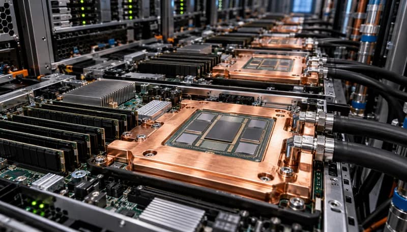
Addressing these microscopic heat fluxes mandates direct-to-chip (D2C) liquid cooling operating with optimized microchannel geometries. Advanced cold plates feature specialized copper or silicon micro-fins (channel widths <50 μm, aspect ratios >10:1) positioned directly over known silicon hot spots to induce turbulent local fluid dynamics. Furthermore, conventional phase-change Thermal Interface Materials (TIM1/TIM1.5) suffer rapid thermal degradation, voiding, and pump-out under cyclic thermomechanical stresses generated by differential thermal expansion across disparate die materials. System architects must implement liquid metal alloys (such as Gallium-Indium-Tin) or sintered silver paste layers to maintain the total thermal junction-to-fluid resistance ($R_{th, j-f}$) below 0.05 K/W.
Localized heat flux management: Dissipate continuous hotspot thermal fluxes exceeding 150 W/cm² while preserving silicon junction temperatures below 85°C.
TIM material reliability: Deploy high-performance liquid metal (bulk thermal conductivity >30 W/m·K) or sintered silver to prevent mechanical pump-out under thermal cycling.
Microchannel fluid optimization: Engineer cold plate microchannel fin pitches to sub-50 μm dimensions, maximizing turbulent boundary layer thermal transfer.
Server Platform and Rack-Level Densification: Power Distribution Busbars, 54V Power Shelves, and Open Rack (ORV3) Mechanical Constraints
At the server platform and rack level, the transition to high-power chiplet sockets fundamentally disrupts mechanical form factors and power distribution paradigms. Standard 19-inch rack geometries running legacy 12V distribution face fatal electrical efficiency penalties: a standard 100 kW rack running at 12V would require 8,333A flowing across the backplane, incurring massive $I^2R$ resistive copper losses and requiring physically unmanageable copper busbar volumes. Under modern Open Compute Project Open Rack Standard V3 (ORV3) specifications, hyperscalers have unified infrastructure around a centralized 48V/54V DC busbar topology, reducing current flows by a factor of 4.5 and lowering resistive distribution losses by over twentyfold.
ORV3 architecture concentrates power distribution into dedicated 1OU/2OU Power Shelves populated with Titanium-grade power supply units (PSUs) achieving peak conversion efficiencies exceeding 96.5%. The server sleds interface with the solid copper backplane busbar via spring-loaded blind-mate connectors. Concurrently, these sleds integrate mechanical liquid cooling manifolds with drip-free Quick Disconnect (QD) couplings. The integration of high-mass copper cold plates, internal fluid loops, and heavy multi-layer server motherboards imposes severe mechanical constraints, demanding reinforced rack chassis designs that accommodate dynamic chassis deflection limits under static compute sled loads exceeding 40 kg per node.
Busbar electrical topology: Standardize rack power backplanes on 48V/54V DC rails to reduce distribution conductor mass and constrain $I^2R$ power losses.
PSU efficiency benchmarks: Mandate 80 PLUS Titanium-certified power conversion modules exhibiting ≥96.5% peak electrical efficiency at 50% load.
Mechanical loading limits: Engineer ORV3 compute sled chassis and rack frames to resist flexure and deflection tolerances below 2 mm under maximum populated weight.
Hyperscale Facility Infrastructure Engineering: Transitioning Brownfield White Space to Support 60kW-120kW Liquid-Cooled Chiplet Racks
The deployment of chiplet-based compute architectures drives hyperscale rack power envelopes from legacy air-cooled parameters (10 kW to 20 kW per rack) to sustained densification levels between 60 kW and 120 kW+ per rack. Supporting these extreme power footprints requires comprehensive retrofitting of brownfield white space and redefining greenfield facility designs. Raised-floor air distribution systems fail completely at these densities due to fan power scaling laws, acoustic limits, and airflow volume limits. Hyperscale facilities must migrate to closed-loop hydronic networks driven by internal or end-of-row Cooling Distribution Units (CDUs) managing primary and secondary fluid loops.
Facility secondary loops must be engineered to comply with the ASHRAE Liquid Cooling Class W4 standards, which permit cooling fluid inlet supply temperatures ranging up to 45°C. Operating at W4 parameters eliminates the capital expenditure and high parasitic power consumption of mechanical refrigerant chillers, enabling 100% dry cooler or evaporative economizer operation across virtually all global climatic zones. By decoupling white space cooling from complex refrigeration compressors, hyperscalers can achieve Power Usage Effectiveness (PUE) targets below 1.15 at full 120 kW rack density. Hydraulic engineering mandates rigorous real-time monitoring of differential pressure, biocide dosing, and flow balancing (typically requiring 1.0 to 1.5 LPM per kilowatt of rejected thermal load) to ensure continuous operation.
Cooling distribution: Implement secondary loop CDUs supporting liquid mass flow rates between 1.0 and 1.5 liters per minute per rejected kilowatt of rack load.
ASHRAE W4 thermal envelopes: Operate secondary loop fluid supply temperatures at up to 45°C to achieve chillerless facility designs with PUE < 1.15.
Facility hydraulic balancing: Maintain strict differential pressure stability (±5 kPa) across parallel cold plate circuits using automated variable-frequency pump arrays.
Engineering Procurement & Technical Desk
For technical datasheets, custom power topology design, or volume export quotations, reach out to HEFENGQI engineers.